- Published on
Live JTAG on the BD Alaris 8015
- Authors

- Name
- Chris Wheeler

- Name
- Charlotte Steinichen
- Name
- Sean Carrick
- Name
- Prashant Anantharaman
This post documents the hardware reverse engineering of the BD Alaris 8015 infusion pump. Prior public work on the Alaris 8015, most notably Rapid7's medical-device research,1 recovered the firmware only by destructively desoldering the NOR flash and reading it on an external programmer, without ever establishing on-chip debug access. By tracing the JTAG lines to the J1 connector and halting the PXA270 over a standard debugger, we brought up live, non-destructive debug access to the device, something that prior published teardowns never achieved.
The engagement was conducted under the ARPA-H UPGRADE program, a multi-institution medical-device cybersecurity initiative. The objective was to obtain a complete binary image of the device firmware and to identify on-board debug access points for dynamic analysis.
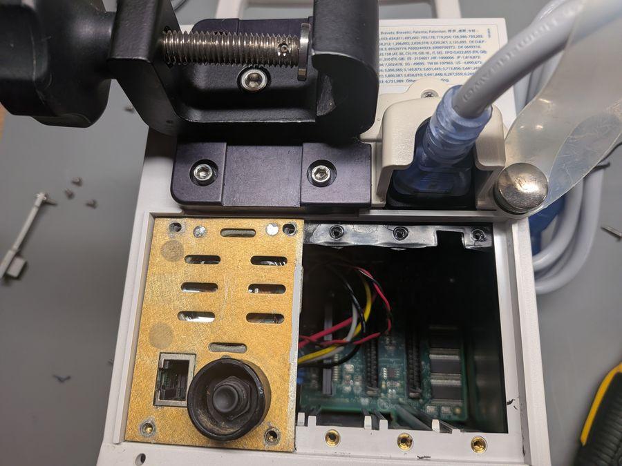
Several physical Alaris 8015 units were used during this work. The flash extraction was performed on one device. Chip-inventory photography and JTAG continuity tracing were performed on a second sample of the same logic board design. The live JTAG bring-up was performed on a third, working unit. Destructive procedures and live-target procedures were deliberately separated across boards.
Target device
The Alaris 8015 PCU (Point of Care Unit) is the processing and control unit of a large-volume IV infusion pump. It is an FDA 510(k)-cleared medical device used in clinical settings to meter intravenous drugs into patients. The unit operates from a measured 23.9 V supply provided by its power module.
Component identification
All major integrated circuits were identified under a stereo microscope, with markings read directly from each package. Five parts are relevant to this writeup.
| Component | Part number | Package |
|---|---|---|
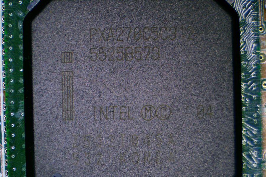
| Processor | Intel PXA270C5C312 | 23x23 mm, 360-ball PBGA |
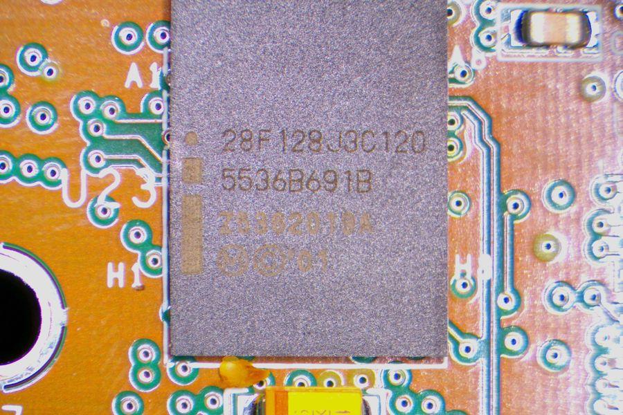
| NOR flash | Intel 28F128J3 (128 Mbit) | BGA64 |
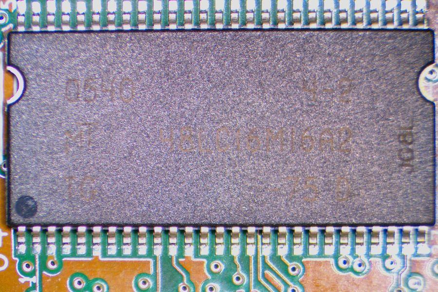
| SDRAM | Micron MT48LC16M16A2 (256 Mbit, x16) | TSOP-II |
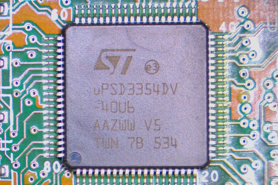
| MCU with PSD | ST uPSD3354DV-40U6 | 80-pin LQFP |
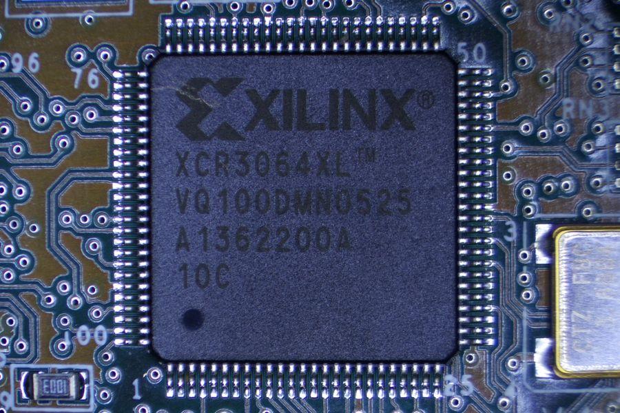
| CPLD | Xilinx XCR3064XL-10VQ100 | 100-pin VQFP |
The PXA270 is an XScale (ARMv5TE) application processor. The XScale and PXA product lines were originally Intel parts and were sold to Marvell in 2006, so the same device appears under both manufacturer names depending on the datasheet revision.
On another Alaris PCU, we found that the MCU was TI MSP430F5418A, and not the ST microcontroller.
Locating the debug interface
Three of the identified chips contain JTAG TAP controllers: the Intel PXA270, the STMicroelectronics uPSD3354DV, and the Xilinx XCR3064XL CPLD. The first task was to determine where their JTAG lines terminate.
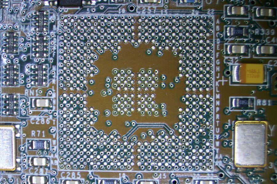
GTRI performed X-ray imaging of the 12-layer PCB and reported that the JTAG signals for all three chips route to a single 50-pin internal board-to-board connector designated J1. This was corroborated by Figure 7-24 of the Alaris Technical Service Manual. On a 12-layer stackup the JTAG traces run predominantly on inner layers, so X-ray imaging was the practical method for following them.
JTAG signal tracing
To verify and refine the X-ray findings, continuity testing was performed on a spare board. The PXA270 was desoldered so that each JTAG ball location became an open pad that could be probed directly, and continuity from those pads to J1 was measured with a multimeter.
Per the PXA270 datasheet (Order No. 280002-006), the JTAG balls are located in the lower-right quadrant of the 360-ball package: TCK at R19, TMS at R20, TDO at R21, TDI at R22, and nTRST at T20. Continuity testing produced the following mapping.
PXA270 to J1 (right side):
| Signal | PXA270 ball | J1 pin | Notes |
|---|---|---|---|
| TDO | R21 | 7 | Via 75 ohm series resistor R81 ("75R0") |
| nRESET | W20 | 8 | Direct |
| TCK | R19 | 9 | Direct |
| TMS | R20 | 10 | Direct |
| TDI | R22 | 11 | Direct |
| nTRST | T20 | 12 | Direct |
The TDO path required attention. It runs through a 75 ohm series resistor (R81), so a direct continuity test between the ball and J1 pin 7 reads as no connection. The resistor must be probed across for the route to be detected.
uPSD3354DV to J1 (right side). JTAG is on the chip's Port C per ST datasheet 9685 Rev 7:
| Signal | Chip pin (LQFP80) | J1 pin |
|---|---|---|
| TMS | 20 (PC0) | 13 |
| TCK | 16 (PC1) | 14 |
| TDI | 7 (PC5) | 17 |
| TDO | 6 (PC6) | 18 |
| RESET_IN | 68 | 19 |
Xilinx XCR3064XL to J1 (left side). Pin assignments per Xilinx DS017:
| Signal | Chip pin (VQ100) | J1 pin |
|---|---|---|
| TMS | 15 | 3 |
| TCK | 62 | 4 |
| TDI | 4 | 5 |
| TDO | 73 | 6 |
The CPLD presents one constraint. Its PORT_EN pin (VQ100 pin 11) measured 100 ohm to ground, and the datasheet specifies that PORT_EN must be held high to enable JTAG functionality; when low, those pins operate as user I/O. PORT_EN is not exposed at J1, so the CPLD chain may require that pin to be forced high before it will respond.
Power and ground on J1 were identified as VCC_IN (3.3 V) on right pin 1, measured at 3.25 V, and GND on left pin 1, at chassis ground. Each chip has its own dedicated TCK, TMS, TDI, and TDO signals at J1. The chips are not daisy-chained, so each TAP is addressed independently.
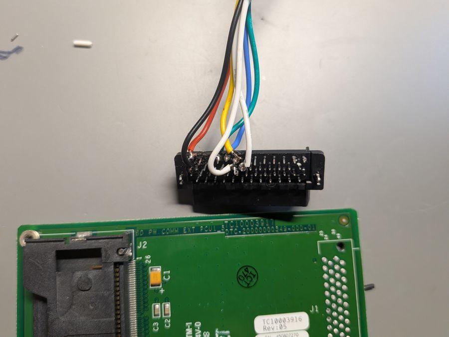
Constructing a JTAG harness
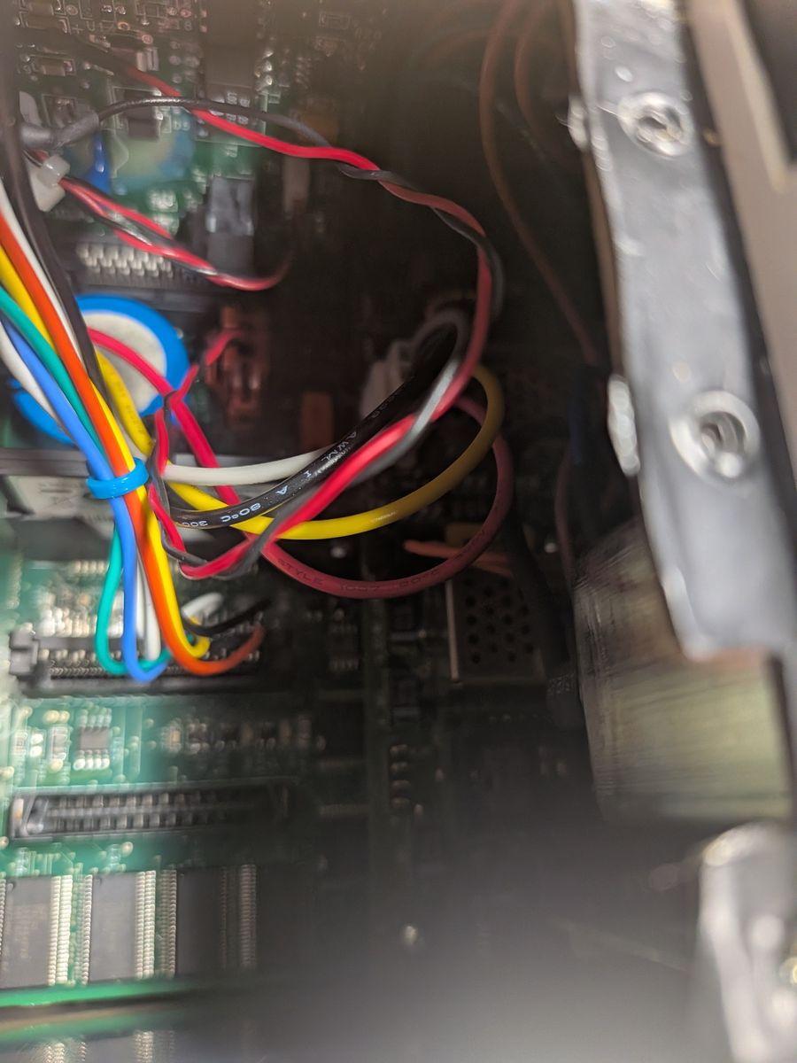
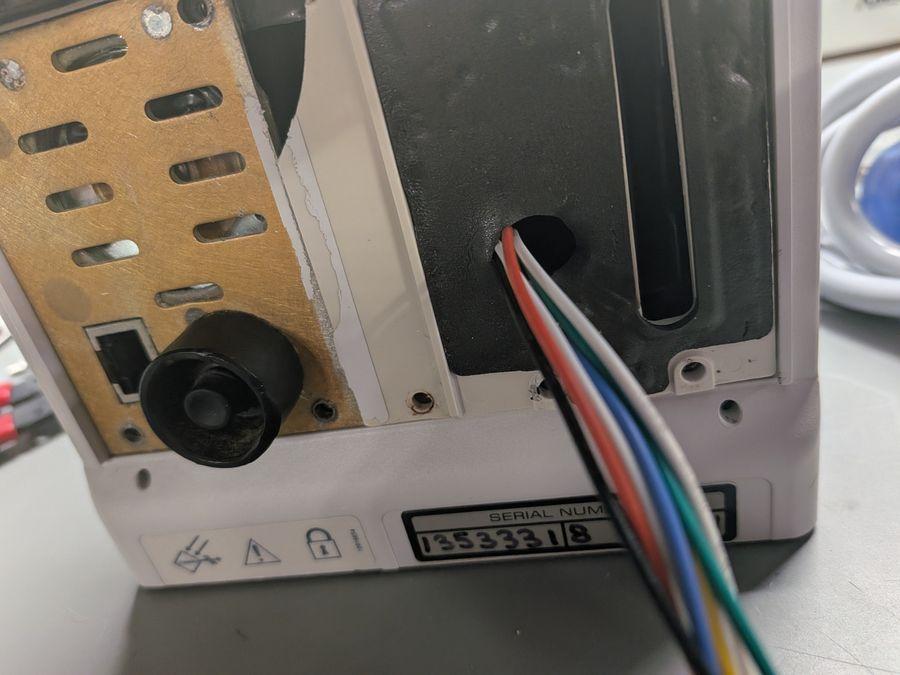
J1 is an internal board-to-board connector with no readily available mating part. An identical 50-pin connector was salvaged from an internal WiFi card daughter board located adjacent to J1 inside the unit. The salvaged connector was hot-air desoldered from the daughter board, and color-coded cables were soldered directly to the relevant pins to bring the JTAG signals out to a flying breakout.
| Signal | J1 pin | Cable color |
|---|---|---|
| GND | Left 1 | Black |
| VCC_IN (3.3 V) | Right 1 | Red |
| TDO | Right 7 (via R81 75 ohm) | Green |
| nRESET | Right 8 | Yellow with black stripe |
| TCK | Right 9 | Blue |
| TMS | Right 10 | White |
| TDI | Right 11 | Yellow |
| nTRST | Right 12 | White with black stripe |
JTAGulator verification
Before connecting the primary debug adapter, the harness wiring was independently verified with a JTAGulator configured for a 3.3 V target supply, scanning channels 0 through 4.
JTAG> j
Enter starting channel [0]: 0
Enter ending channel [4]: 4
Possible permutations: 120
...
TDI: 2
TDO: 1
TCK: 4
TMS: 3
Device ID #1: 0111 1001001001100101 00000001001 1 (0x79265013)
TRST#: 0
JTAG combined scan complete.
IDCODE 0x79265013 decodes as JEDEC manufacturer 0x009 (Intel), part 0x9265, version 0x7. This is one of the three valid PXA270 IDCODEs recognized by OpenOCD's stock pxa270.cfg target configuration; the other two, 0x49265013 and 0x89265013, correspond to different silicon steppings. A clean scan with all four signals identified confirmed that the harness wiring and pin mapping were correct.
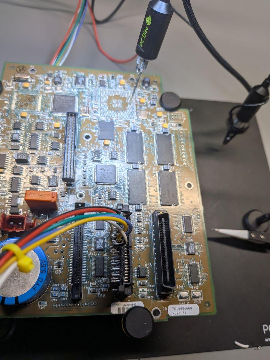
JTAG bring-up with the J-Link Pro
With signaling confirmed, the breakout was connected to a Segger J-Link Pro V5 through a generic 20-pin ARM JTAG board, using the following assignments.
| J-Link pin | Signal | Connected to |
|---|---|---|
| 1 | VTref | VCC_IN (3.3 V) |
| 3 | nTRST | J1 right 12 |
| 4 | GND | J1 left 1 |
| 5 | TDI | J1 right 11 |
| 7 | TMS | J1 right 10 |
| 9 | TCK | J1 right 9 |
| 13 | TDO | J1 right 7 |
| 15 | nSRST | J1 right 8 (PXA270 nRESET) |
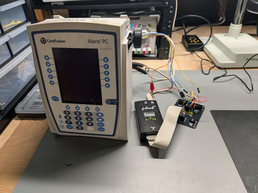
One compatibility issue is worth noting. Current versions of Segger's J-Link Commander no longer support the PXA270, as the PXA family was removed from Segger's device database. OpenOCD 0.12.0, which retains an XScale target driver, was used instead. The configuration was as follows.
adapter driver jlink
transport select jtag
adapter speed 1000
reset_config trst_and_srst srst_open_drain
source [find target/pxa270.cfg]
The stock pxa270.cfg defines the PXA270 TAP with IR length 7, expects one of the three known IDCODEs, and configures reset timing (adapter srst delay 260, jtag_ntrst_delay 250) together with the PXA270's internal SRAM at 0x5C000000 as the work area. With OpenOCD running, the reset init command was issued over the telnet interface on port 4444, and the CPU halted at the reset vector.
> reset init
JTAG tap: pxa270.cpu tap/device found: 0x79265013
    (mfg: 0x009 (Intel), part: 0x9265, ver: 0x7)
target halted in ARM state due to debug-request,
    current mode: Supervisor
cpsr: 0xd80000d3  pc: 0x00000000
MMU: disabled, D-Cache: disabled, I-Cache: disabled
A program counter of 0x00000000 with the MMU and both caches disabled indicates a clean halt at the reset vector, with no firmware code yet executed. This provides the baseline state required for dynamic analysis of the bootloader and main application. From this state, the full 16 MB firmware image can be read over JTAG with the OpenOCD command dump_image flash_jtag.bin 0x00000000 0x1000000.
Firmware analysis summary
An initial analysis of the JTAG-acquired image using static string extraction, entropy analysis, binwalk signature scanning, and the ARM exception vector table produced the following layout. No region exceeded an entropy of 7.5, indicating that the firmware is not encrypted.
| Region | Size | Contents |
|---|---|---|
| 0x000000 to 0x10FFFF | approx. 1.06 MB | Bootloader |
| 0x140000 to 0x4FFFFF | approx. 3.75 MB | Log storage |
| 0x500000 to 0x5FFFFF | 1 MB | FlashFX filesystem |
| 0x600000 to 0xDCCA93 | approx. 7.80 MB | Main application ELF |
The bootloader carries the internal codenames "Polo" (BSP) and "Tequila" (board), a polo@tequila> shell prompt, and version 12.1.0.76 built on December 8, 2019. It is based on Enea OSE 5.1.0 with the Interpeak networking stack and OpenSSL 0.9.7c. The main application, "Pcu1.5App" version 12.1.3.6 built on April 6, 2022, is a statically linked ARM ELF with a load address of 0xA0100000, also based on Enea OSE with the Interpeak IPNET stack and OpenSSL 1.0.1g. Identified strings include process names, protocol handlers (DCMP with AES, NCM and PTP protobuf references, FTP, TFTP, and Telnet), and a full set of WiFi security strings ranging from WEP through WPA2-EAP-TLS.
Our second device contained the same "Polo" bootloader and "Pcu1.5App" versions, but included an older Enea OSE 4.5.2.
Conclusion
Starting from a sealed device, the team identified the major silicon, used GTRI X-ray imaging to locate a buried 50-pin debug connector, confirmed its pinout by desoldering the processor and verifying continuity on every JTAG line, constructed a working harness from a salvaged connector, and halted the PXA270 at its reset vector using a Segger J-Link Pro driven by OpenOCD's XScale target driver. From that halted state the full 16 MB firmware image can be read directly over JTAG. Together these results establish a foundation for dynamic analysis of the device.
Acknowledgements
Charlotte Steinichen is at GTRI (Georgia Tech Research Institute), and Brendan Saltaformaggio is the principal investigator of the H-VIPER project.
X-ray imaging of the 12-layer logic board was performed by GTRI (Georgia Tech Research Institute).
This work was performed as part of the ARPA-H UPGRADE program's H-VIPER project led by the Georgia Tech Research Corporation under Contract No. 140D042590046. The views, opinions, and/or findings expressed are those of the author(s) and should not be interpreted as representing the official views or policies of ARPA-H or the U.S. Government.